JPWC 1812

JPWC1812
JPWC1812
Application:
Notebook, PC's, USB, HUB, Consumer Electronics, Internet of things
Feature
  • Common mode choke with magnetic shield.
  • Excellent solder ability and resistance to soldering heat.
  • High reliability and easy surface mount assembly.
  • Low DC resistance , high current tolerance and stable performance.
More information
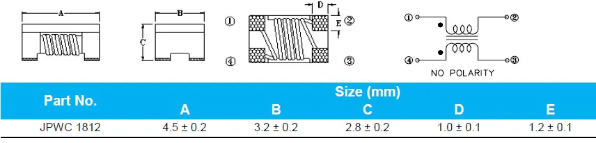
Shape and Dimensions


Showing 1 to 12 of 12 items
Inquiry
View Picture Add to Product View Picture P/N Impedance (Ω)at 100MHz RDC (Ω) Max. IDC (mA) Max. Rated Volt.(Vdc) Max. Withstand Volt.(Vdc) Max. Insulation Resistance(Ω) Max. Datasheet (.pdf)
JPWC 1812-900/2, JPWC1812-900/2 JPWC 1812-900/2, JPWC1812-900/2
90±25%
0.05
2000
50
125
10M
JPWC 1812-201/1.5, JPWC1812-201/1.5 JPWC 1812-201/1.5, JPWC1812-201/1.5
200±25%
0.10
1500
50
125
10M
JPWC 1812-601/1.5, JPWC1812-601/1.5 JPWC 1812-601/1.5, JPWC1812-601/1.5
600±25%
0.24
1500
50
125
10M
JPWC 1812-801/1, JPWC1812-801/1 JPWC 1812-801/1, JPWC1812-801/1
800±25%
0.24
1000
50
125
10M
JPWC 1812-142/1, JPWC1812-142/1 JPWC 1812-142/1, JPWC1812-142/1
1400±25%
0.24
1000
50
125
10M
JPWC 1812-900/4, JPWC1812-900/4 JPWC 1812-900/4, JPWC1812-900/4
68 min.
90 typ.
0.05
4000
50
125
10M
JPWC 1812-231/3.5, JPWC1812-231/3.5 JPWC 1812-231/3.5, JPWC1812-231/3.5
173 min.
230 typ.
0.05
3500
50
125
10M
JPWC 1812-421/3.2, JPWC1812-421/3.2 JPWC 1812-421/3.2, JPWC1812-421/3.2
300 min.
420 typ.
0.055
3200
50
125
10M
JPWC 1812-601/2.5, JPWC1812-601/2.5 JPWC 1812-601/2.5, JPWC1812-601/2.5
450 min.
600 typ.
0.06
2500
50
125
10M
JPWC 1812-901/2.3, JPWC1812-901/2.3 JPWC 1812-901/2.3, JPWC1812-901/2.3
650 min.
900 typ.
0.07
2300
50
125
10M
JPWC 1812-142/2, JPWC1812-142/2 JPWC 1812-142/2, JPWC1812-142/2
1000 min.
1400 typ.
0.10
2000
50
125
10M
JPWC 1812-282/0.9, JPWC1812-282/0.9 JPWC 1812-282/0.9, JPWC1812-282/0.9
2100 min.
2800 typ.
0.35
900
50
125
10M